The fluorescent hum of a server farm, miles away from the C-suite theatrics, is where the real battle for silicon supremacy is fought. It’s in the meticulous, often maddening, process of silicon design, where a single misplaced transistor can derail months of work and billions in investment.
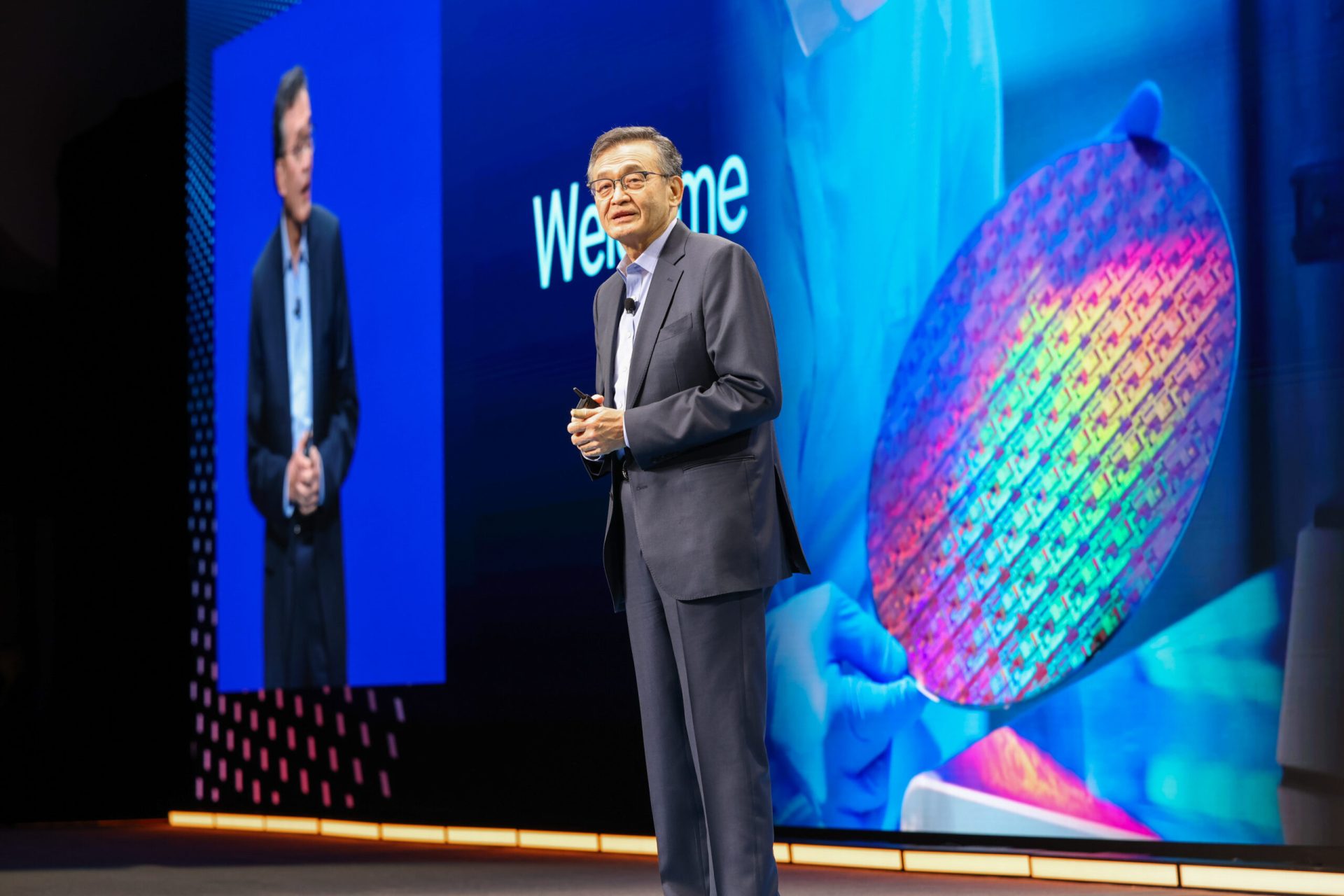
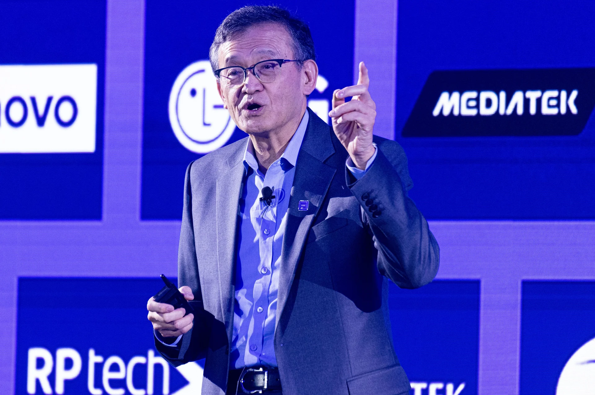
And now, Intel’s CEO, Lip-Bu Tan, has apparently decided to inject a potent, some might say terrifying, dose of urgency into that process. His new directive, delivered with the starkness of a battlefield order, essentially says: miss your early production targets, and you’re out. Specifically, any chip design that requires more than a couple of revision cycles – landing beyond B0 stepping – is grounds for termination. It’s a culture shift, he admits, something Intel seemingly lacked. This isn’t just about speed; it’s about a fundamental rethinking of how Intel, and by extension its foundry business, approaches product development. Tan calls this aggressive stance a necessary cultural implant, designed to instill a discipline of hitting critical early milestones, starting with tape-out (A0) and pushing through to B0 with minimal fuss.
The B0 Ultimatum: A Ruthless Push for Efficiency
During a recent appearance, Tan laid out his new doctrine with unnerving clarity: “I have a culture right now, I just implemented. I have to be A0 to production. Now, A0 is when you tape out first-time parts. And Intel don’t have that culture.” He followed this with the kicker: “So I kind of said, well, first-time part, A0. B0, you keep your job. Anything above that, you’re fired. So that culture people initially thought that I’m just joking.” It’s a bold, and for engineers, likely terrifying, move. Gone are the days, it seems, of iterative fixes stretching into double-digit revision numbers and endless delays. The implication is stark: designs must be near-perfect out of the gate, or the architects face the consequences. This high-stakes gamble is designed to streamline the painfully long lead times that have plagued Intel for years, a stark contrast to the agile, rapid-iteration cycles seen at rivals like TSMC.
This isn’t just about internal discipline; it’s a clear signal to Intel’s foundry customers. They’re looking for predictability, for roadmaps that are more than just wishful thinking. Tan understands this implicitly. “People don’t go to you just one node,” he explained. “They’re looking for the roadmap for the future. So we have to build a long-term business.” And a long-term business, in this hyper-competitive foundry landscape, demands reliability and a demonstrably efficient path from concept to volume production.
“So I kind of said, well, first-time part, A0. B0, you keep your job. Anything above that, you’re fired. So that culture people initially thought that I’m just joking.”
The 14A ‘Holy Grail’: A Glimpse of the Future
Amidst this internal shake-up, Intel is also pushing forward on its next-generation process technologies. The 14A node, which Tan dubs the “Holy Grail,” is targeted for risk production in 2028 and volume production in 2029. Crucially, this timeline puts it in direct competition with TSMC’s anticipated A14 process, both touted as 1.4nm technologies. This head-to-head race is far more than a technical skirmish; it’s a critical indicator of which foundry can deliver cutting-edge manufacturing at scale when the market demands it most. Talks with major customers, including titans like Apple and TeraFab, underscore the high stakes. The progress on the 14A’s Process Design Kit (PDK) is also on track, with the 0.9 PDK slated for external customer release in October 2026. For internal teams, that timeline is even tighter.
Beyond 14A, Intel is already charting its course for the even more advanced 10A (1.0nm) and 7A (0.7nm) nodes. While roadmaps are still nascent, the industry’s trajectory points towards an inevitable push into sub-nanometer territory, a frontier where TSMC is also investing heavily. Intel’s ambition here isn’t just to catch up, but to reclaim a leadership position, particularly in advanced packaging solutions and novel substrate technologies like glass, slated for rollout by 2030. This multifaceted approach—combining leading-edge nodes with sophisticated packaging—is the company’s gambit to win long-term foundry partnerships. They’re not just selling a single manufacturing process; they’re selling a vision for the future of chipmaking.
Why This Matters: Beyond the Hype
Lip-Bu Tan’s aggressive stance on product revisions is more than just a management tactic; it’s an architectural imperative. The industry has reached a point where the complexity of silicon design, coupled with the immense cost of fabrication, demands an almost pathological commitment to getting it right the first time. Traditional chip development cycles, often characterized by protracted debugging and multiple re-spins, are becoming economically untenable, especially as we stare down the barrel of single-nanometer process nodes. This is where the true ‘holy grail’ lies – not just in shrinking transistors, but in streamlining the process of creating them. Tan’s threat of termination for exceeding B0 stepping is, in essence, a blunt instrument to enforce architectural rigor and engineering discipline. It’s a signal that Intel’s foundry business isn’t just about manufacturing capacity; it’s about manufacturing precision and predictability. In an era where AI accelerators and advanced compute architectures demand increasingly complex and error-free designs, this relentless focus on early-stage stability is the bedrock upon which future silicon innovation will be built.
Is Intel’s New Policy Just Corporate Theater?
It’s easy to dismiss Tan’s pronouncements as typical CEO bluster, meant to energize a workforce and impress investors. But a closer look at Intel’s foundry ambitions—particularly its race against TSMC in the sub-1nm era and its push into advanced packaging—suggests a deeper, more structural shift is at play. The demand for substrates is already outstripping supply, a clear indicator that the industry is bottlenecked upstream. Tan’s mandate, while draconian, addresses a known pain point: design delays due to unforeseen issues late in the development cycle. If Intel can genuinely instill this culture of discipline, it could provide a significant competitive advantage in a foundry market that prizes speed and reliability. The real test, of course, will be in its sustained execution and whether it leads to actual improvements in first-pass success rates and reduced time-to-market, rather than just a wave of firings and a demoralized engineering staff.
What Does A0 vs. B0 Stepping Mean for Chip Design?
In chip design, ‘stepping’ refers to a revision or iteration of a silicon design. A0 is typically the first functional tape-out – the initial version of the chip’s layout sent for manufacturing. B0 is the next revision. While revisions are normal and often necessary to fix bugs or optimize performance, a large number of steppings (like going all the way to, say, E0 or F0) indicates significant design issues that are proving difficult and time-consuming to resolve. Tan’s policy aims to drastically curtail this, forcing engineers to resolve most critical issues within the A0 to B0 transition. This means designs must be exceptionally well-validated and understood before they enter the manufacturing process, reducing costly delays and uncertainty.
🧬 Related Insights
- Read more: NVIDIA OpenShell: Sandboxes for AI Agents That Actually Work?
- Read more: TSMC Packaging Test: MediaTek Denies Intel Link
Frequently Asked Questions
What does it mean if a chip design exceeds B0 stepping? Exceeding B0 stepping means a chip design has undergone multiple revisions beyond the initial tape-out (A0) and the first significant iteration (B0). Intel CEO Lip-Bu Tan’s policy states that designs requiring further revisions beyond B0 could lead to job termination for the responsible personnel.
When will Intel’s 14A process technology be available? Intel’s 14A process technology, which CEO Lip-Bu Tan calls the ‘Holy Grail,’ is slated for risk production in 2028 and volume production in 2029. The 0.9 PDK for external customers is expected in October 2026.
Will Intel’s strict policy affect its ability to compete with TSMC? Tan’s policy is intended to enhance Intel’s competitiveness by improving efficiency and reducing development time. If successful, it could lead to more predictable product cycles and greater customer confidence. However, the draconian nature of the policy also risks alienating engineering talent if not managed effectively.