So, we’re building chips that are basically tiny supercomputers, right? Millions, billions of transistors crammed onto a sliver of silicon, all thanks to this thing called IP—intellectual property. But here’s the kicker: every single piece of that IP, from the simplest logic gate to the most complex memory block, needs to be meticulously characterized. Think of it as getting a detailed personality profile for every tiny component before you put them all together. And with design nodes shrinking to 3nm and 2nm, the amount of data we’re talking about? It’s astronomical. Engineers are already drowning in SPICE simulations, spending weeks just to get the basic timing models—the .lib files—that dictate how these chips actually perform. It’s become the digital equivalent of watching paint dry, only the paint is incredibly expensive and failure means a multi-million dollar re-spin.
Now, Siemens EDA, bless their hearts, they’ve decided enough is enough. They’ve rolled out an expanded version of their Solido Characterization Suite, slapping some AI on it and calling it a day. The promise? To finally drag library characterization kicking and screaming into the 21st century. They’re talking about replacing those agonizing manual, schedule-busting cycles with some fancy generative and agentic AI workflows. Sounds great on paper. The real question, as always, is who’s actually going to benefit, and how much will it cost us?
Is This AI-Powered Approach Actually Faster?
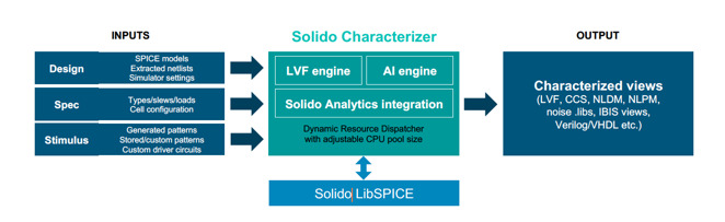
At the core of this new gizmo is the Solido Characterizer. Siemens is flogging a 7x throughput increase, a number that’ll make any project manager nod approvingly. They’re achieving this by mashing together two things: an AI-driven engine and something they’re calling Solido LibSPICE. Apparently, this LibSPICE is built specifically for this kind of library IP, giving a 2x+ speed boost on its own. Pair that with their advanced LVF (Liberty Variation Format) tricks—which claim a 5x speedup—and you’re supposedly shaving a significant chunk off the simulation phase. GlobalFoundries, one of the early guinea pigs, is apparently happy, saying it maintains production accuracy while speeding things up. I’ll believe it when I see my own chip designs finish in days instead of weeks.
But the real magic, or so they say, happens with Solido Generator. This is where the machine learning comes in, building an analytical model of a library from just a few key data points—the “anchor” PVT corners (Process, Voltage, Temperature). Once trained, this thing can churn out new .libs in minutes, not weeks. We’re talking 100x faster than SPICE. This is their new methodology for multi-corner libraries. Instead of SPICE-ing every single variation, Generator uses reinforcement learning to smartly model the whole space, hitting the crucial accuracy spots while skimping on the less important ones. It claims to support all the standard formats, so your signoff-ready models should be, you know, actually ready.
Why Does Data Accuracy Matter So Much?
Speed is one thing, but if the data’s garbage, the speed is pointless. At these advanced nodes, tiny errors can snowball into catastrophic failures. Traditional checks, the kind that have been around forever, often miss subtle glitches in LVF data. These glitches can apparently mess with your chip’s timing by 100% or more at 3nm. Siemens says Solido Analytics uses fancy visualization and AI to sniff out these issues—things that old-school methods just can’t see. They even let you visualize things like standard deviation and skewness, which sounds incredibly useful if you’re into that sort of thing. Because honestly, staring at raw simulation logs is about as fun as a root canal.
And it’s not just for the characterization folks. The Solido Library Profiler is supposed to help the physical design teams. They can actually compare Power, Performance, and Area (PPA) of different libraries early in the design process. No more kicking off a massive Place & Route job only to find out the library you picked was a dud. This profiler uses some kind of “smart auto-alignment” to map differences down to the pin and arc level. If it actually works, that alone could save design teams a mountain of wasted time and resources.
But here’s the real kicker, the bit that ties it all together: the Fuse EDA AI system. This is where the generative and agentic AI magic supposedly happens. It’s supposed to offer a more dynamic debugging experience, pointing out issues, watching runs, and even suggesting re-runs to keep things moving. Think of it as a really, really smart assistant for your characterization engineers. It’s this integration that makes the whole suite feel like it’s actually moving beyond just faster simulations to a fundamentally different way of working. And with the ability to scale out to thousands of CPUs in the cloud, Siemens is clearly positioning this not as a nice-to-have, but as an essential lifeline to keep the semiconductor roadmap from collapsing under its own weight.
Who is Actually Making Money Here?
Let’s cut through the noise. Siemens EDA is selling a solution to a problem they, and the entire industry, have been wrestling with for years. Foundries need faster characterization to get their IP out the door. Chip designers need accurate libraries to build competitive products. Every week shaved off the characterization cycle translates directly into faster time-to-market, which, in this cutthroat business, is everything. The AI itself isn’t the product; it’s the engine that drives the value proposition. The value is in reduced engineering hours, fewer failed tape-outs, and ultimately, getting that new smartphone or server chip into consumers’ hands sooner. Siemens is selling efficiency, plain and simple, wrapped in the shiny new packaging of AI. And if their claims hold water, they’re going to make a pretty penny doing it.
“The era of manual, schedule-volatile characterization is ending, replaced by generative and agentic AI workflows.”
That quote from Siemens’ own PR is the core of their pitch. It’s bold. It’s a declaration of war on the status quo. And frankly, it’s overdue. The sheer complexity of modern chip design demands new approaches. Whether this AI-powered suite is the silver bullet or just another incremental improvement remains to be seen. But one thing’s for sure: the old ways of doing things just aren’t cutting it anymore.
🧬 Related Insights
- Read more: ZSNES reborn: GPU powers ultimate accuracy
- Read more: Prebuilt PC Deal: RTX 5060 Ti Rig Under $1500
Frequently Asked Questions
What does Solido Characterization Suite actually do?
It’s a set of tools designed by Siemens EDA to speed up and improve the process of creating and validating detailed models (.lib files) for semiconductor IP used in chip design. It uses AI to make these simulations and verifications much faster and more accurate.
Will this AI replace chip characterization engineers?
Siemens suggests these tools will augment engineers’ capabilities, making them more productive rather than replacing them. The AI handles repetitive, time-consuming tasks, allowing engineers to focus on more complex problem-solving and verification.
How much faster is this compared to traditional methods?
Siemens claims significant speedups, citing up to 7x faster throughput for initial characterization and over 100x faster generation of library models using machine learning. Specific components of the suite offer individual speed improvements that combine for the overall gain.