Samsung Hits 900 Layers.
The relentless march towards denser flash memory, measured by stacking layers of NAND cells vertically, has a new frontrunner. Reports indicate Samsung Electronics has developed a 900-layer-class V-NAND prototype, a move that significantly ups the ante in a critical segment of the semiconductor industry. For context, this isn’t just a marginal improvement; it’s a substantial leap past the roughly 200-300 layers common in consumer devices and even the ~300-500 layer technology driving high-end enterprise solutions. This kind of advancement is where real market dominance is forged.
Is Samsung Actually Winning the NAND Race?
This prototype isn’t a shipping product, and the devil, as always, resides in the details of yield, cost, and performance at scale. However, the announcement — or rather, the leak — itself is telling. It forces competitors, notably China’s YMTC, to react and potentially accelerate their own roadmaps. The layered approach is fundamental to NAND flash density. Each layer represents an opportunity to cram more data into the same physical footprint, driving down per-gigabyte costs and enabling the ever-increasing storage demands of data centers, AI training systems, and our mobile devices. Samsung’s reported progress suggests they’ve effectively navigated the considerable engineering hurdles involved in stacking so many layers without compromising signal integrity or durability.
The market dynamics here are stark. In a capital-intensive industry like semiconductor manufacturing, being first with a breakthrough technology can confer significant competitive advantages, including market share, pricing power, and the ability to set new industry standards. While YMTC has been making aggressive strides, particularly with its Xtacking technology that aims to simplify interconnects, Samsung’s layered approach, if successful at 900 layers, would demonstrate a different, potentially more established, path to high density. The narrative Samsung is pushing is one of sustained, incremental, but ultimately decisive, innovation in manufacturing process.
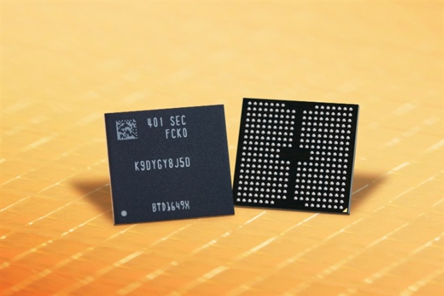
Samsung Electronics appears to be pulling ahead. The South Korean chipmaker has reportedly developed a 900-layer-class V-NAND prototype, a significant leap that underscores its leadership in next-generation memory technology.
The sheer complexity of manufacturing such a device at scale cannot be overstated. We’re talking about etching, deposition, and lithography processes that must be executed with atomic-level precision across hundreds of layers, each one separated by microscopic conductive and insulating materials. Failures at any stage can render entire chips unusable. This is why Samsung’s reported success is noteworthy; it implies a mastery of these incredibly challenging manufacturing techniques. The company’s long history in V-NAND development, moving from 32-layer to 48, 64, 96, 128, and now reportedly into the 900-layer class, paints a picture of relentless investment and process refinement.
Why Does This Matter for Data Centers and AI?
The implications for the data center and AI industries are profound. These sectors are voracious consumers of storage, requiring high-capacity, high-speed solutions. As AI models grow exponentially in size and complexity, the ability to store and quickly access massive datasets becomes a critical bottleneck. Higher layer counts in NAND directly translate to more terabytes per drive, lower latency for data retrieval, and ultimately, reduced total cost of ownership for storage infrastructure. If Samsung can bring 900-layer NAND to market efficiently, it could set a new benchmark for storage performance and density, accelerating the pace of AI development and deployment. It’s not just about more storage; it’s about making that storage smarter, faster, and more accessible.
The geopolitical undercurrents are also impossible to ignore. In an era where supply chain resilience and technological sovereignty are paramount, a nation-state backed entity like YMTC challenging established players like Samsung, SK Hynix, and Micron becomes a significant strategic consideration for governments worldwide. Samsung’s purported leap in layer count, if confirmed and productized, serves as a powerful counter-narrative against concerns about competitive stagnation or reliance on single-source technologies. It’s a demonstration of the core capabilities that underpin global technological leadership.
What’s Next for NAND?
The ultimate question is whether this 900-layer prototype is a true stepping stone to mass production or a showcase of engineering prowess that remains years away from commercial viability. Industry analysts will be scrutinizing Samsung’s future announcements for details on yield rates, power efficiency, and endurance metrics. The performance characteristics of these ultra-high-layer count NAND flash devices will be key. Will they offer the same level of endurance and reliability as current generations, or will compromises be necessary? The memory industry’s history is littered with ambitious prototypes that never quite made it to the mainstream. However, given Samsung’s track record and the sheer market pressure, it’s highly probable that this 900-layer development is more than just a research exercise. It’s a signal.
The competitive pressure doesn’t end with YMTC. SK Hynix, Micron, and Kioxia are all investing heavily in their own multi-layer NAND technologies. The race isn’t just about hitting a certain layer count; it’s about achieving it at a competitive cost and with superior performance characteristics. This means continuous innovation in materials science, etching technology, and 3D integration. We’re entering an arms race where the prize is not just market share, but the very foundation of the digital economy.
🧬 Related Insights
- Read more: Renesas Buys Vision AI Firm: Is Your MCU Smarter Now?
- Read more: AI Achieves Formal Verification Milestone [Chip Design]
Frequently Asked Questions
What does 900-layer V-NAND mean? It signifies that the NAND flash memory chip is constructed by stacking 900 individual layers of memory cells vertically, allowing for significantly higher storage density compared to previous generations.
Will this make my phone storage bigger? Eventually, yes. While prototypes aren’t consumer products, advancements like 900-layer NAND eventually trickle down to consumer devices, enabling larger storage capacities in smartphones, laptops, and other electronics at potentially lower per-gigabyte costs.
How does Samsung’s 900-layer NAND compare to competitors? Samsung’s reported 900-layer prototype is a significant jump, reportedly surpassing the layer counts currently in mass production by competitors like YMTC and others in the industry. However, actual commercial product performance and cost will be the ultimate differentiators.