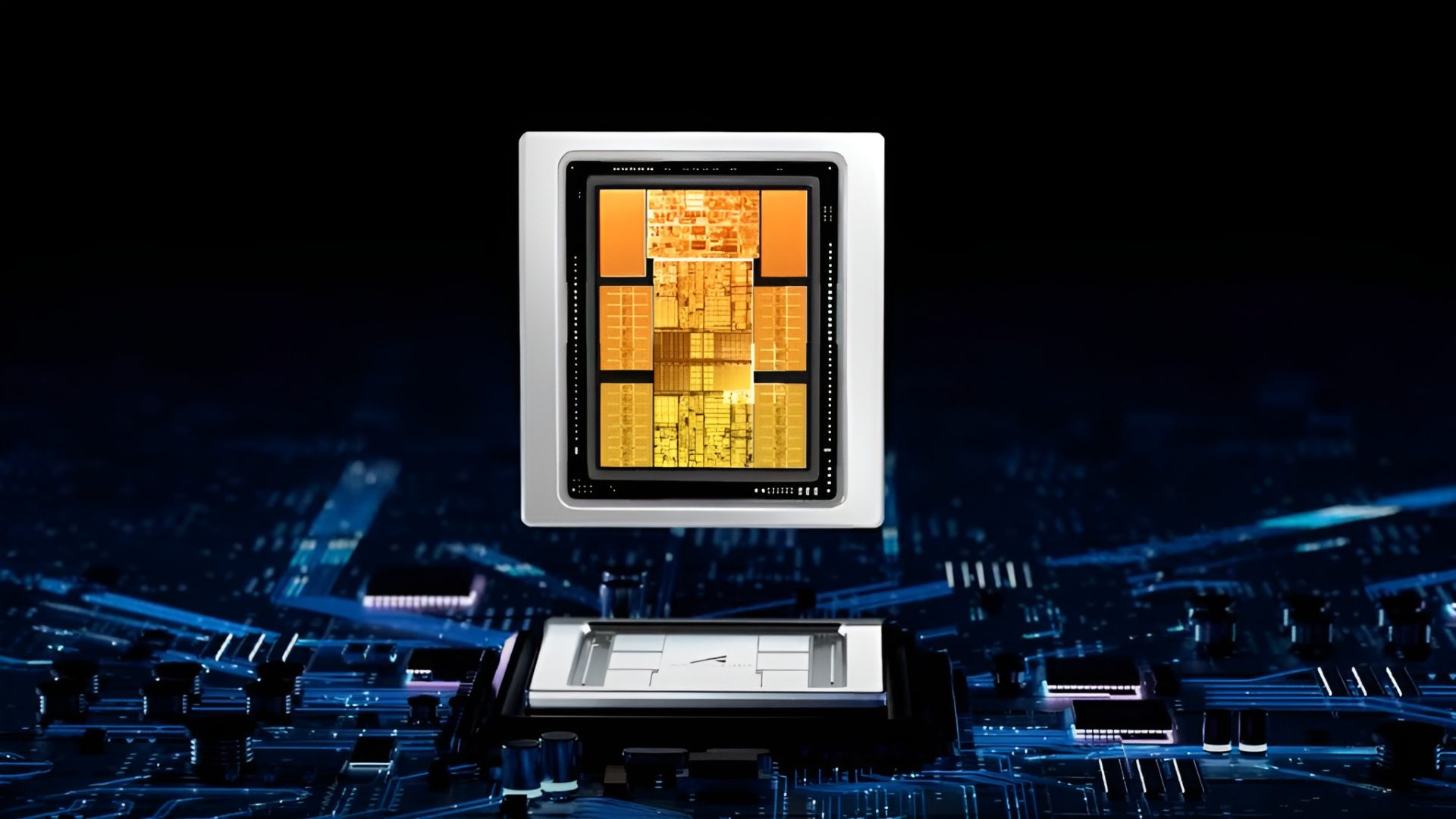
Forget about the dry spec sheets and corporate jargon for a moment. What does this mean for your phone, your laptop, the very fabric of the digital world humming around us? It means the race to cram more power into smaller spaces isn’t just continuing; it’s morphing. Huawei, facing down sanctions that have slammed the door shut on its access to cutting-edge chip-making tools, is pushing back. They’re not just trying to keep up; they’re claiming to be redefining the very rules of the game, a move that’s got the semiconductor world buzzing with both admiration and a healthy dose of skepticism.
The Great Reframe: Is It a New Law, Or Just a New Name?
So, Huawei rolls out this concept called ‘Tau scaling,’ and suddenly, they’re talking about transistor density that rivals industry leaders like TSMC and Intel. Sounds impressive, right? Like a classic underdog story, a David vs. Goliath moment in the silicon arena. But hold on your horses. Top chip analyst Dr. Ian Cutress isn’t exactly doing a victory lap. His take? It’s less about breaking new ground and more about skillfully sidestepping the old. He points out, quite rightly, that Huawei’s announcement seems to be comparing apples and oranges – lumping together disparate performance metrics rather than sticking to the established playbook.
And get this – the research paper outlining this ‘Tau scaling’? Cutress suspects it might have been AI-assisted. That’s a whole other layer of fascinating complexity, isn’t it? AI writing about AI-adjacent tech, trying to outmaneuver geopolitical roadblocks. Wild.
Moore’s Law, that venerable pillar of the tech world, has long been our North Star, promising twice the transistors every couple of years. But for Huawei, shackled by those US sanctions cutting them off from the holy grail of EUV (Extreme Ultraviolet) lithography, that star is out of reach. So, their strategy, as Cutress lays it out, is to simply… change the destination. “We need to redefine what our goals are,” they’re essentially saying. “And their argument is that we’re gonna redefine this by ignoring Moore’s Law, because we can’t compete with that.” It’s a bold pivot, a strategic pivot, if you will, away from direct competition on transistor density and towards… well, something else.
Cutress frames it as Huawei trying to redefine performance by looking at the whole system, the chip, and other components. The density of transistors, in this view, becomes less important. It’s a clever argument, certainly, but is it a redefinition or a refocusing? Cutress leans towards the latter. “You’re not redefining the view. You’re refocusing the view,” he states. It’s like saying you’re reinventing the wheel when you’re actually just changing the tire pressure. Still important, still impactful, but not quite the radical overhaul the announcement might suggest.
Beyond Density: The Tangible Tech of Tomorrow
This isn’t just academic musing. What Huawei is hinting at – and what companies like Intel and AMD have been quietly perfecting for years – is advanced packaging. Think of it like building a skyscraper instead of just a bigger apartment. Instead of stuffing more rooms into one floor (higher transistor density on a single die), you start stacking floors, or even connecting multiple buildings efficiently. This is where technologies like hybrid bonding and chip-on-chip stacking come into play.
AMD’s presentation from 2021, as Cutress highlights, already showed the nascent reality of stacking chips. This concept, however, has been brewing for a decade or more. Intel’s EMIB (Embedded Multi-die Interconnect Bridge) technology, for instance, connects multiple chiplets side-by-side, offering a way to build powerful processors without relying on a single, impossibly large and complex piece of silicon. Hybrid bonding is the next step, a more intimate connection that removes the older, bulkier microbumps, allowing for incredibly tight connections.
But here’s the rub – the sheer complexity. As you try to connect these stacked chips with ever-finer pitches (the distance between connections), you run into a wall of physics. Resistance, capacitance – they all increase, demanding more power and limiting clock speeds. The dream of nanometer-level pitches is tantalizing, but moving from a lab demonstration to mass production? That’s the chasm. “The biggest problem between research and productization, is moving it into volume. Cause you can do it once in a lab, fine, doing it ten million times in a facility, is, problematic.” A very human observation, that. Manufacturing at scale is where dreams often meet the unforgiving reality of physics and economics.
Furthermore, the energy cost of this advanced packaging is staggering. Cutress points to ASML’s hybrid bonding solutions, which require ten times more energy per square centimeter than leading-edge EUV transistors. This means slower production, higher costs, and a harder path to achieving good yields – those precious, error-free chips that make it out of the factory.
“Now as you go down, you need finer and finer and finer pitches. You need smaller and smaller micron sized pitches. And the reason why that is, is because every time you go over these connections, you encounter resistance and capacitance. And you have to overcome that. And the way you overcome that is by more and more connections running at lower and lower frequency.”
So, Huawei’s ‘Tau scaling,’ which seems to encompass these advanced packaging techniques alongside other optimizations, isn’t necessarily a new scientific principle. It’s more of a strategic integration and re-framing of existing, albeit cutting-edge, technologies. It’s a way to extract more performance and density without the very specific lithography tools that are off-limits.
The AI Angle: A Double-Edged Sword?
And that AI paper? It’s a whisper that grows louder. If AI is indeed helping to craft the research, it speaks volumes about the accelerating role of AI in R&D. It also raises questions about genuine human innovation versus sophisticated AI-driven optimization. It’s a fascinating, and perhaps slightly unnerving, glimpse into the future of scientific discovery. Is this a sign of AI augmenting human intellect, or beginning to replace it? For now, it’s a tool, a powerful one, but the underlying human ingenuity (or lack thereof, depending on your perspective) is what’s truly at play.
Ultimately, Huawei’s announcement is a proof to human resilience and ingenuity in the face of adversity. It’s a strategic maneuver, a redefinition of what it means to be at the cutting edge when the conventional path is blocked. While Dr. Cutress might not be ready to rewrite the history books just yet, the fact that Huawei is pushing the boundaries in any way, and forcing the industry to rethink its metrics, is undeniably a significant development. It’s a reminder that innovation isn’t always a straight line; sometimes, it’s a wild, unpredictable zigzag.
🧬 Related Insights
- Read more: Boris Cherny’s Claude Code Workflow: Five AIs, One Terminal, Infinite Output
- Read more: TSMC Bonus Fury: 58% Profit Jump Sparks Strike Threats
Frequently Asked Questions
What does Huawei’s Tau scaling actually do? Huawei’s Tau scaling technology focuses on improving chip performance and transistor density by optimizing the entire system, including advanced packaging techniques like chip-on-chip stacking and hybrid bonding, rather than solely relying on traditional lithography advancements.
Will Huawei’s new technology work without EUV lithography? Huawei aims to achieve advanced transistor densities and performance improvements by leveraging other technologies, effectively sidestepping the need for the EUV lithography equipment that is currently unavailable to them due to US sanctions. This redefines how chip performance is measured and achieved.
Is Huawei truly redefining Moore’s Law? According to analysts like Dr. Ian Cutress, Huawei is more reframing or refocusing the discussion around chip performance rather than fundamentally redefining Moore’s Law itself. They are adapting their strategy to achieve competitive results given their manufacturing constraints.