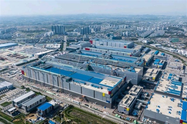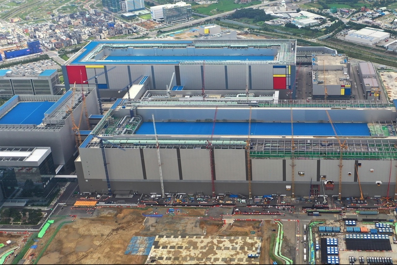
The whispers are growing louder, and they’re coming from Pyeongtaek, South Korea. Samsung Electronics, a titan of the semiconductor world, is reportedly charting a course that could send seismic waves through the global DRAM market. Come 2027, much of its crucial P4 cleanroom capacity, the very engine for high-volume memory production, is slated to be re-tooled for next-generation High Bandwidth Memory (HBM).
This isn’t just a minor production tweak; it’s a strategic pivot. Think of it like a chef deciding to dedicate their entire prime kitchen space to crafting exotic, niche dishes, leaving fewer burners available for everyday staples. The implication is stark: a tightening supply of general-purpose DRAM, the workhorse memory that powers everything from your laptop to your server farm.
The AI Gold Rush and its Ripple Effect
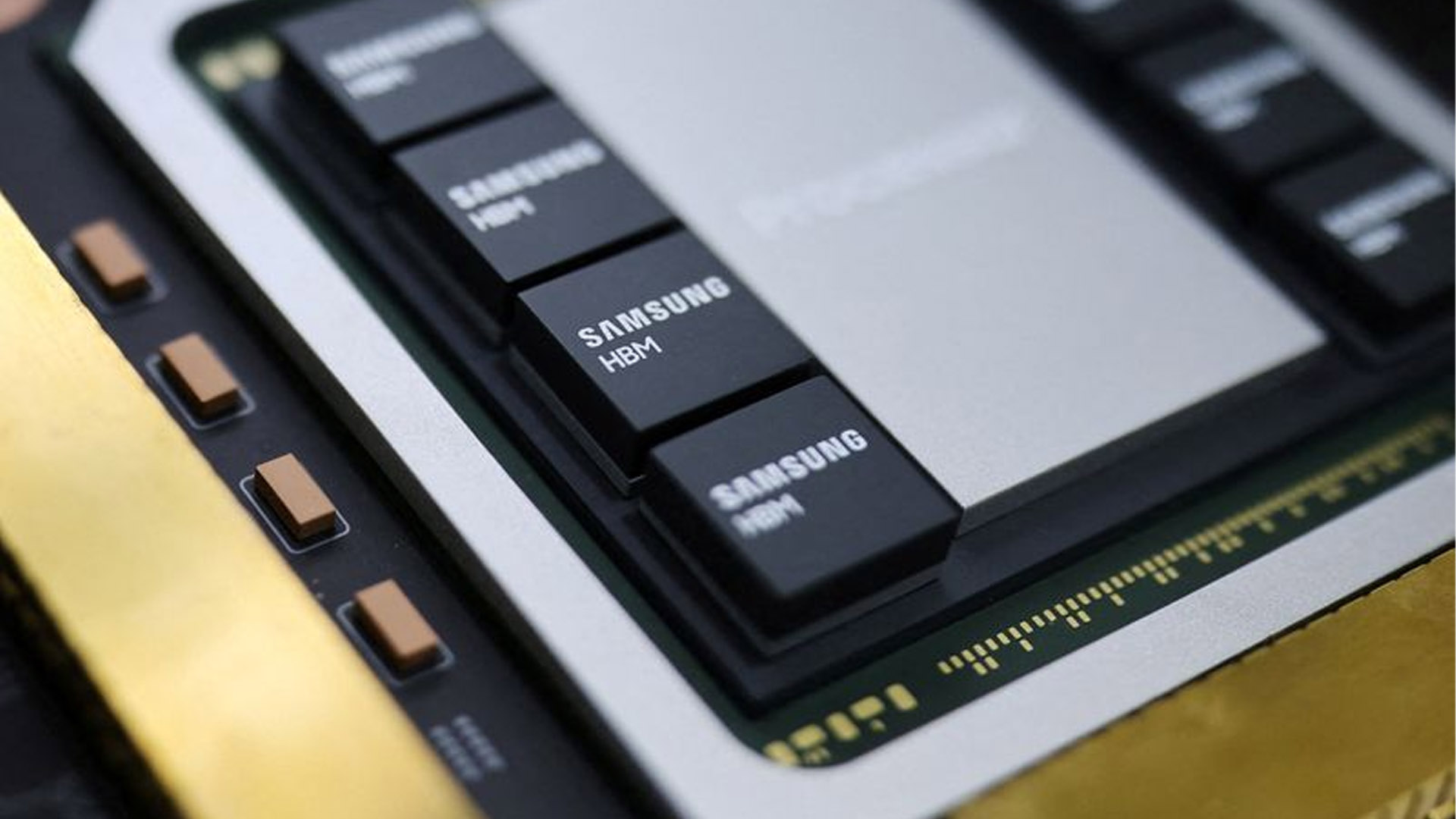
What’s driving this seismic shift? Look no further than the insatiable appetite for AI acceleration. HBM, with its stacked architecture and vastly superior bandwidth, is the undisputed king of memory for AI accelerators like NVIDIA’s GPUs. As the AI race intensifies, demand for HBM is skyrocketing, forcing memory manufacturers into a difficult calculus. Do they invest heavily in the hot new thing, or ensure a steady supply of the foundational tech? Samsung, it seems, is placing its bets squarely on the former.
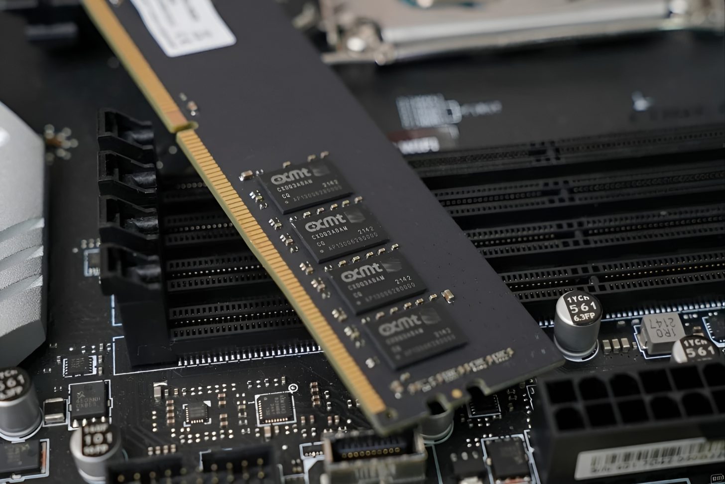
This strategic allocation means less capacity for the more commoditized, albeit essential, DDR5 and older DRAM modules. For consumers and businesses relying on these chips, the story is simple: higher prices and potential shortages are on the horizon. It’s a classic supply-and-demand narrative, amplified by the sheer scale of Samsung’s manufacturing footprint.
Pushing the Envelope, or Playing with Fire?
The architecture of HBM itself is what makes it so desirable for AI. Instead of just lining up DRAM chips on a board, HBM stacks them vertically, using through-silicon vias (TSVs) to create incredibly short, high-speed connections. This allows for massive amounts of data to be fed to the AI processors with unparalleled efficiency.
Samsung’s P4 facility, a massive undertaking in the memory manufacturing landscape, represents a significant chunk of their advanced process technology. Shifting this considerable capacity to HBM production isn’t a small undertaking. It requires re-tooling, recalibrating, and a deep commitment to a technology that, while booming now, could face its own evolving challenges down the line. The company isn’t just responding to current demand; it’s making a long-term play on the future of high-performance computing.
But here’s the thing that keeps me up at night: This isn’t happening in a vacuum. Other memory giants like SK Hynix and Micron are also pouring resources into HBM. While competition is generally good, a coordinated push into a single, specialized memory type from multiple major players simultaneously could create a bottleneck for the broader DRAM market that’s hard to rectify quickly. It feels like the industry is collectively leaning over a cliff, and we won’t know if there’s a net on the other side until we’re already falling.
“We are investing heavily in HBM to meet the soaring demand from the AI sector. This strategic shift will position us as a leader in the next generation of memory solutions.”
That’s the official line, of course. And it’s not entirely wrong. Samsung will likely cement its leadership in the HBM space. But the real question is at what cost to the rest of the semiconductor ecosystem? This move is less about a simple capacity adjustment and more about Samsung betting big on the AI future, potentially at the expense of the present.
The Hidden Costs of Specialization
The historical parallel here isn’t exact, but it evokes memories of previous industry pivots where specialization led to unforeseen market imbalances. When foundries focused too heavily on one type of chip, it often created vacuums elsewhere. The current HBM push, while driven by a legitimate and colossal demand, carries similar risks. The world still needs its general-purpose DRAM, and the lead times for building new, dedicated DRAM fabs are immense.
This could create a significant crunch in 2027, especially if AI demand continues its exponential climb and other sectors of the economy don’t see a corresponding slowdown. We’re talking about the foundation of digital infrastructure here. A shaky foundation, built on a scarcity of essential components, can have far-reaching consequences – from stunting the growth of nascent AI applications to impacting the affordability of consumer electronics. It’s a delicate dance, and Samsung’s aggressive move is a particularly forceful step.
Will This Replace Your Job?
While the immediate impact will be on manufacturing capacity and pricing, the long-term implications could touch various roles within the tech industry. For developers, it might mean more focus on memory optimization for AI workloads. For hardware engineers, it’s a call to innovate on DRAM architectures or explore alternative memory technologies. For supply chain managers, it’s a complex puzzle of securing components. It’s less about job replacement and more about a significant shift in focus and required skill sets.
FAQ
What is Samsung’s P4 facility? Samsung’s P4 facility in Pyeongtaek, South Korea, is a significant manufacturing plant for memory semiconductors, particularly its advanced DRAM production lines.
Why is HBM important for AI? HBM offers significantly higher bandwidth and lower power consumption compared to traditional DRAM, making it ideal for feeding the massive data requirements of AI accelerators like GPUs.
When will the DRAM crunch potentially happen? Reports suggest the impact on DRAM supply could become most pronounced around 2027, coinciding with Samsung’s major capacity shift to HBM.